Saturday 29 October 2011

Microprocessor(8085/8086) Question bank


Question Bank
Microprocessor and its Application (EC-307)
B.Tech, 5th Semester ECE
Introduction to Microprocessor
Marks: 2 each
1. List the components of a computer
2. Explain the function of each component of a computer.
3. What is a Microprocessor? What is the difference between a Microprocessor & CPU?
4. Define bit, byte, word, double word, quad word and instruction
5. What determines that Microprocessor is an 8, 16 or 32 bit?
6. Explain the difference between the machine language and the assembly language of
the 8085 microprocessor.
7. What is an assembler?
8. What are low and high level languages?
9. What are the advantages of an assembly language in comparison with high level
languages?
10. List the four operations commonly performed by the MPU.
11. Specify the four control signals commonly used by the 8085 MPU.
12. Specify the function of the address bus and the direction of the information flow on
the address bus.
13. Why is the data bus bidirectional?
14. What is a bus?
8085 Microprocessor
Marks: 2 each
15. How many memory locations can be addressed by a microprocessor with 14 address
lines?
16. How many address lines are necessary to address two megabytes (2048K) of
memory?
17. Why is the data bus bidirectional?
18. Specify the control signal and the direction of the data flow on the data bus in a
memory-write operation.
19. What is the function of the accumulator?
20. What is a flag?
21. Why are the program counter and the stack pointer 16-bit registers?
22. What is the function of the WR signal on the memory chip?
23. Specify the number of registers and memory cells in a 128 x 4 memory chip.
24. What is the memory word size required in an 8085 system?
25. While executing a program, when the 8085 MPU completes the fetching of the
machine code located at the memory address 2057H, what is the content of the
program counter?
26. What is the role of clock in Microprocessor?

Marks: 5 each
27. What is the difference between INR & INX instructions?
28. List all the interrupt signals of 8085 microprocessor.
29. Write short note on evolution of microprocessors.
30. Explain the functions of the ALE and IO/M signals of the 8085 microprocessor.
31. List the sequence of events that occurs when the 8085 MPU reads from memory.
32. If the 8085 adds 87H and 79H, specify the contents of the accumulator and the status
of the S, Z, and CY flags.
33. If the clock frequency is 5 MHz, how much time is required to execute an instruction
of 18 T-states?
34. Discuss the programming model of 8085 μP with the help of suitable diagram.
35. Draw and explain the timing diagram for opcode fetch operation
36. Discuss various types of addressing modes of 8085.
37. Explain why the number of output ports in the peripheral-mapped I/O is restricted to
256 ports.
38. In the peripheral-mapped I/O, can an input port and an output port have the same port
address? Explain.
39. What are the control signals necessary in the memory-mapped I/O?
40. List the four categories of 8085 instructions that manipulate data.
41. Define opcode and operand, and specify the opcode and the operand in the instruction
MOV H, L.
42. Write logical steps to add the following two Hex numbers. Both the numbers should
be saved for future use. Save the sum in the accumulator. Numbers:
A2H and 18H.
Marks: 10 each
43. (a)Specify the contents of the registers and the flag status as the following
instructions are executed.
i. MVI A, 00H
ii. MVI B, F8H
iii. MOV C, A
iv. MOV D, B
v. HLT
(b)Write instructions to load the hexadecimal number 65H in register C and 92H in
accumulator A. Display the number 65H at PORT0 and 92H at PORT1.
44. Draw and explain the block diagram of a microprocessor 8085.
45. (a)Why the lower order address bus is multiplexed with data bus? How they will be
de-multiplexed?
(b) Differentiate between maskable and non-maskable interrupts.
46. Write an 8085 assembly language program using minimum number of instructions to
add the 16 bit no. in BC, DE & HL. Store the 16 bit result in DE pair.
47. (a)Explain in detail the following instructions:-
(i) ADC (ii) LHLD (iii) RLC (iv) DI
(b) Define & explain the term addressing modes.
8086 Microprocessor
Marks: 2 each
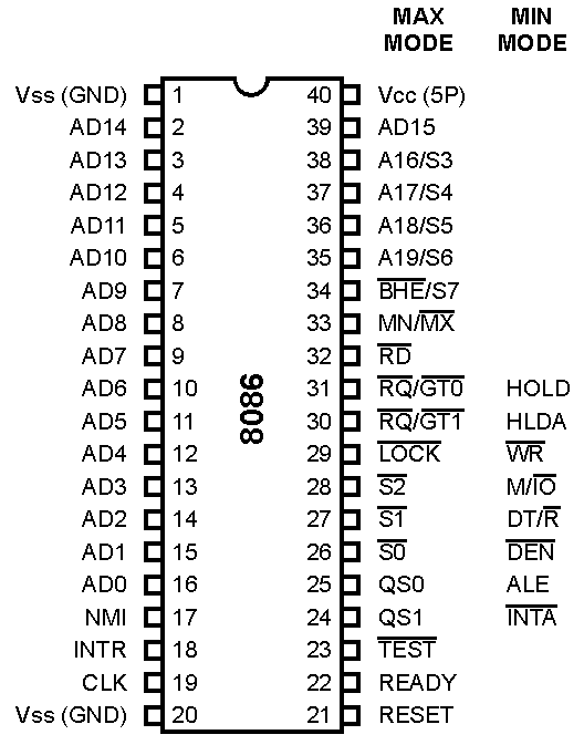
48. What are important signals of Intel 8086?
49. How many operating modes does 8086 have?
50. How many functional units does 8086 contain?
51. What is the function of a segment register in 8086?
52. What are conditional and control flags in 8086?
53. How many interrupt lines does 8086 have?
54. What physical address is represented by:
(i) 4370 : 561E H (ii) 7A32 : 0028 H
55. Describe the difference between the instructions:
(i) MOV AL, 0DB H (ii) MOV AL,DB H
Marks: 5 each
56. Briefly explain the maximum mode configuration of 8086.
57. What is the difference between minimum and maximum modes of 8086?
58. How many interrupts are available in 8086? List the predefined software interrupts
available in 8086.
59. Briefly explain the maximum mode configuration of 8086.
60. What is the purpose of MN/Mx pin? Explain.
61. Explain the concept of segmented memory? What are its advantages?
62. Explain the concept of pipelining in 8086. Discuss its advantages and disadvantages.
Marks: 10 each
63. Discuss the interrupt system of Intel 8086. What is interrupt pointer? What is 'type' of
an interrupt?
64. Discuss the various addressing modes of 8086. What are displacement, base and
index? What is an effective address or offset?
65. What is the difference between minimum and maximum modes of 8086? How are
these modes selected?
66. Draw and explain the architecture of 8086.
67. Write an 8086 program to add two 16-bit numbers in CX and DX and store the result
in location 0500H addressed by DI.
Microprocessor system peripheral and interface
Marks: 5 each
68. What is interfacing?
69. Explain the concept of Direct Memory Access (DMA).
70. Explain the functions of Handshake signals.
71. Explain what SIM is. Discuss the bit pattern of the accumulator for SIM instruction.
72. List the operating modes of the 8155A programmable device.
73. Write a note on any of the applications of microprocessors.
Marks: 10 each
74. Explain the DMA controller 8257?
75. Draw the block diagram of 8255 and explain its working. What is Control Word?
Determine the control word for the following configuration of 8255:-
Port A – Output
Mode of port A – Mode 1
Port B – Output
Mode of port B – Mode 0
Port C lower (pins PC0 – PC2) – Output
76. What is 8254? Discuss its various operating modes. What are its areas of
applications?
77. Explain major components of 8259 with the aid of suitable diagram.
78. Explain USART in detail.
79. Explain the functional diagram of keyboard and display controller.
80. Explain the functional diagram of 8155 and explain its control word.

8086 Microprocessor


Introduction:
8086 microprocessor is introduced in 1978 by intel co. and adopted by IMB for their PC in 1981. The intel 8086 is 16 bit, N-channel, HMOS(High speed - MOS) microprocessor, It consumes less power and draws 360mA current on 5V supply.8086 is manufactured for standard temperature range 32F to 180F as well as extended temp. range 40F to 225F. In market 3 version of 8086 are available
S. No.
Version
Frequency
1.
8086
5 Mhz
2.
8086-1
10 Mhz
3.
8086-2
8 Mhz

It is built on a single-semiconductor chip and packed in 40 pin IC pack, the package is DIP (Dual In-Line Package).It contains an electronic circuit of 29000 transistors. 8086 is the first member of X86 or 80X86 family followed by 8088, 80186, 80188, 80386, 80486 and Pentium names.
Features of 8086 microprocessor:
1.      It is 16 bit microprocessor.
2.      It has 20 address lines, so it can address 220 = 1mb memory locations.
3.      It has multiplexed address and data bus which reduced the no. Of pins needed, but multiplexing slightly slow down the transition of data.
4.      It has 16 control lines for providing handshaking singles during bus transfer and for permitting at least some external control of the CPU.
5.      It requires only one, +5 volt supply voltage.
6.      It supports both multiprogramming and multiprocessing.
7.      Its instruction stream byte queue speed up its execution of instruction.
Pin Description of 8086:
AD0-AD15: (Bidirectional) Address/data lines, these are low order address bus and multiplexed with data.
AD16-AD20: High order address bus multiplexed with status signals.
AD16/S3,AD17/S4: AD16 & AD17 multiplexed with segment identifier signals S3 & S4,
AD18/S5:  AD18 is multiplexed with interrupt status S5,
AD19/S6: AD19 is multiplexed with status signal S6.
BHE /S7 (output): Bus high enable/ status. It is used to enable data onto the most significant half of data bus, D8-D15, 8bit device connected to upper half of the bus use BHE signal. It is multiplexed with status S7.
RD(read) : Signal is used to read operation. It is an output signal and active when low. READY (Input) : The addressed I/O or memory sends acknowledgement through this pin. When high it indicates that the peripheral is ready to transfer.
RESET (Input) :  System is reset. The signal is Active high.
CLK (input) : Clock 5,10 or 8 MHz
INTR(Interrupt Request):
QS1
QS0
OPERATION
0
0
     No operation
0
1
     1st byte of opcode from queue
1
0
     Empty the Queue
1
1
     Subsequent byte from Queue


NMI (Input): Non maskable interrupt request.
TEST (Input) : Wait for test control. When it is low the microprocessor continues execution otherwise wait.
S0, S1, S2 (OUTPUT): Pin no. 26,27,28. Status signals. These signals are connected to the bus controller Intel 8288.The bus controller generates memory and I/O access control signal.
S0
S1
S2
Operation
0
0
0
Interrupt acknowledge.
0
0
1
Read data form I/O port.
0
1
0
Write Data to I/O port.
0
1
1
Halt.
1
0
0
Opcode fetch.
1
0
1
Memory Read.
1
1
0
Memory Write.
1
1
1
Passive state.

LOCK (Output) : Active Low, All interrupts are masked and no hold request is granted.
RQ/GT1 , RQ/GT0 : (Bidirectional) Local bus priority control, other bus ask CPU through these lines to release the local bus.(RQ/GT0 has higher priority than RQ/GT1)
Vcc : Power Supply.                          GND: Ground
Operating modes of 8086:
1.      Minimum Operating Mode:  In this mode 8086 works only as CPU of the System.
2.      Maximum Operating Mode: In this mode issue of I/O peripheral and Memory is included.
Block Diagram of 8086:

BUS Interface Unit (BUI): BUI provides an interface of 8086 microprocessor to the outside world. The BUI is responsible for performing all external bus operations. It provides a 16-bits Bidirectional data bus and 20 bits unidirectional address bus.
Roles of BUI:
1.      It sends out address.
2.      Fetches instruction from memory.
3.      Reads data from the ports and memory.
4.      Write data to ports and memory.
Execution Unit (EU): EU contains control circuitry of the microprocessor and translates the instruction fetched from the memory into a series of actions. The 16 bit ALU of execution unit carries out addition, subtraction, AND, OR, XOR, increment, decrement, complement of the binary numbers.
Instruction Stream Byte Queue:  It is also named as instruction Queue or The Queue. This Queue is a set of 6 registers each can store one byte. While EU decodes and executes the instruction then it does not uses buses, in this time BUI fetches upto six instructions and store these prefetched instruction in this FIFO register set. When EU Ready for next instruction it simply reads the prefetched instruction from the Queue. This is much faster than getting instruction from the memory. But in case of JUMP and CALL instruction Queue must be dumped and reloaded stating from new address.
Note: The process of Fetching next instruction while current instruction executes is called pipelining.
Sequential Memory Organization: 8086 microprocessor has 220 = 1,048,576 = 1 Mb locations. Each having 1,048,576 addresses represents a byte wide locations, A 16-bit word will be stored in two consecutive locations. If the 1st word has even address, 8086 can read entire word in one operation and if address is odd then 8086 reads 1st byte with one bus operation another with 2nd bus operation.
MEMORY SEGMENTS: Memory of 8086 is divided into 4 segments each of 64kb within the 1Mb memory space. Each segment represents 64kb consecutive memory location.
Each Segment is assigned a base address that identifies the starting address of the segment.
SEGMENTS ARE:
1.      CODE SEGMENT(CS)
2.      DATA SEGMENT(DS)
3.      EXTRA SEGMENT(ES)
4.      STACK SEGMENT(SS)
Merits of Memory Segmentation :
1.      It facilitates the separate memory area for a program, its data, and the stack.
2.       It facilitates the Multiprogramming and multitasking.
3.      It permits a program and/or its data to be put into different areas of memory each time the program is executed.
4.      Memory capacity becomes 1 mB even through the addres associated with the individual instruction are only 16 bit long.
Registers of 8086:
1.      General Purpose Register (GPR): There are 4 16 bit GPR ( AX, BX, CX, DX) further divided into two 8 bit register.
16 bit Register
8 bit High Order Register
8 bit Low Order Register
AX
AH
AL
BX
BH
BL
CX
CH
CL
DX
DH
DL

2.      Pointer and Index Register: There are two pointer and two index register in 8086.
a.      Stack Pointer (SP)
b.      Base Pointer (BP)
c.      Source Index (SI)
d.      Destination Index (DI)
3.      Segment Registers( CS, DS, ES, SS)
4.      Instruction pointer: It is a 16 bit register and identifies the address of the next instruction to be executed in the code segment. 16 bit content of the IP is called offset or Effective Address (EA).

      Physical Address (PA) = Effective Address (EA) + Code segment (CS)


5.      Status Flag( There are 9 flag register in 8086)


Classification of 8086 Instructions
1.      Data Transfer Instruction: Move, load, store, exchange, input, output, push, and pop are data transfer instruction. For these instructions source and destination may be register, memory and port. e.g.: MOV, XCHG, POP, PUSH etc.
2.      Arithmetic Instruction: Instruction of this group perform addition, subtraction, multiplication division, increment, decrement, comparison, ASCII and decimal adjustment etc. E.g.: ADD, SUB, MUL, DIV, CMP etc.
3.      Logical Instruction: These instructions perform logical operations. E.g.: AND, OR, XOR, NOT and TEST operation. Rotate and shift operation may be included in this group.
4.      Program Execution Transfer (Branch) Instruction: Instruction of this group transfer program execution from the normal sequence to specific destination or target. After the execution of such instruction process start fetching instruction from some new address, rather than continuing same address. E.g. : JMP,JA(JUMP if Above), JAE(JUMP if above or equal),JB(JUMP if Below) JBE, JC, JNC, JNB(JUMP if not Below), JNA etc.
a.      Iteration Control Instruction: Such as LOOP, LOOPE, LOOPZ, LOOPNE, LOOPNZ etc may be included in this group.
b.      Interrupt Instruction: such as INT (Software Interrupt), INTO (Interrupt on Overflow) and IRET (Return form Interrupt Service Subroutine) can also include in this group.
c.      Processor Control Instruction: Instructions of this group are related to flag manipulation and machine control. Example: CLC (Clear Carry Flag), CLD (Clear Direction Flag), CLI (Clear Interrupt Flag) etc.
Addressing Modes of 8086:
There are 8 addressing modes in 8086
Ø      Register Addressing: Operand is placed in a 16 bit or 8 bit register.
                        E.g. : a. MOV AX,BX
                                    b. ADD AL,BL
Ø      Immediate Addressing:  Operand is specified in the instruction itself.
                        E.g.:     a. MOV AL,35H
                                    b. ADD BX,0102H
Ø      Direct Addressing: Operands Offset is given in the instruction itself.
                        E.g.:     a. ADD AL,[0310]
                                    b. ADD AX,[0310]
Ø      Register Indirect Addressing: Operands Offset is placed in any register(BX,BP or SI) specified in the instruction.
                        E.g.:     a. MOV AX,[BX]
                                    b. ADD AL,[SI]
Ø      Based Addressing: Offset of Operand is sum of the content of BX or BP with 8 bit or 16 bit displacement.
            Offset( E.A.) = [ BX + 8 bit or 16 bit Displacement]
                        E.g.:     a. MOV AL,[BX+05]
                                    b. MOV AL,[BX+1346H]
Ø      Index Addressing: Operand’s Offset is sum of content of Index Register(SI or DI) and 8bit or 16 bit displacement.
                        Offset =[SI or DI + 8 bit or 16 bit displacement]
                        E.g.:     a. ADD AX,[SI+05]
                                    b. MOV BX,[DI+1523H]
Ø      Based Indexed Addressing: Offset of operand is sum of Base Register and Index register .
            Offset = [BX or BP] +[SI or DI]
                        E.g.      a. ADD AX,[BX+SI]
                                    b. MOV CX,[BX+SI]
Ø       Based Indexed with Displacement : Offset is given as follows
            Offset = [BP or BX] + [SI or DI] + 8 bit or 16 bit Displacement
                        E.g.:     a. MOV AX,[BX+SI+05]
                                    b. ADD AX,[BX+SI+1234H]